Home Half Term review

We are looking at the evolution of the CPU and memory, the driving factors behind their development and how they are paired.
Central Processing Unit CPU
An important factor to realise about CPUs is they have no real speed, they are rated at a speed, which is in fact the clock speed of the chipset which drives them. The value on the CPU is simply the rating at which it can be clocked without burn out. A processor will happily take faster and faster clocks until the heat generated exceeds the silicon materials rating and it burns out. A way to reduce the heat is to reduce the voltage the core runs at, which in turn means thinner silicon wafer development. This is what developers have been working on since the introduction of the processor some 30 odd years ago.
- Consider how transistors and micron technology improve CPU speed and power.
- What are the physical differences between Slot and Socket CPUs
- Why were CPUs developed in Slot style?
- What are four common Intel CPU types (i.e. pin numbers/Socket or Slot)?
- What are four common AMD CPU types (i.e. pin numbers/Socket or Slot)?
- What are the two Intel P4 pin layouts?
- What is a die?
- What determines how large the die must be?
- What prevents a CPU from being able to clock it faster?
- What is Hyper threading?
- What is ZIF?
- What is LGA? Does it introduce new limitations?
- CPU and FSB relationship.
- Setting the CPU speed on a motherboard.
- A few common CPUs
- A few common Sockets.
- A clocks relationship to power and heat.
- Bus Jargon (Manufacturer's Terminology).
Important concepts to understand
Memory
Getting the right memory for the FSB speed is important to getting a stable operating system. Your motherboard chipset will support more than one FSB setting which gets set by the speed rating of the CPU you buy. This in turn then sets the memory speed you must buy for timing compatibility.
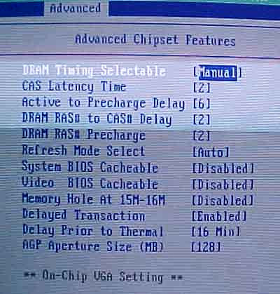
Buying the correct memory DDR400/PC3200 is part of the equation, you must also consider factors like CL (Clock Latency) and Parity (ECC or Non-ECC)
Memory specifications for timings are usually stated such as 2/2/2/6 which relate to the values of the CAS / tRCD / tRP / tRAS These are set in the BIOS and can if set incorrectly cause instability. Most BIOS default settings will be fine provided you have the correct CL (Clock Latency) and Parity (ECC or Non-ECC)
- What is CL?
- Which memory for a 533MHz FSB?
- What is Parity, Registered or ECC?
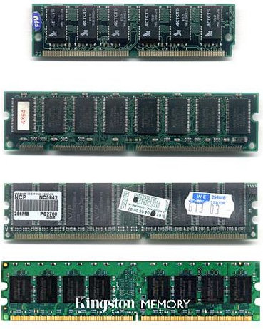
- Identify common memory.
- Match CPU to memory.
- Understand Double Data Rate
Important concepts to understand
Further Reading
Memory timings explained.CPU & Memory Evolution
1995
72-pin SIMM
Approx. 4.25ö x 1ö Has 72 pins on the bottom of the circuit board, 36 on each side. There is a notch cut in the bottom of the circuit board in the middle. These modules measure 4.25 inches long. Because the notch is not centred they can only be put in one way. 72-pin SIMMs are found in older desktop 486 and Pentium computers. Each 72-pin SIMM provides a 32-bit data path, so they can be installed alone in 32-bit systems (486 models) but must be installed in pairs in 64-bit Pentium or AMD Athlon systems. They are available in FPM or EDO.
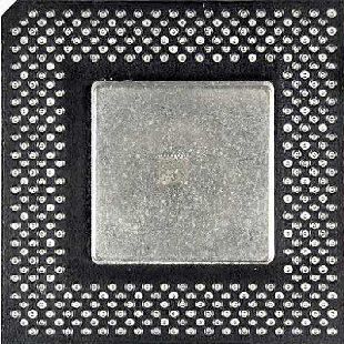
INTEL PENTIUM PRO
Socket 8 387 pins Clock Speed: 133 ¢ 200 MHz Front Side Bus Speed: 60 ¢ 66 MHz L1 Cache: 8KB instruction, 8KB data L2 Cache: 256-1024KB On-Chip. Manufacturing: 0.35 micron. Number of Transistors: 5.5 millions Summary: The first Intel CPU based on the P6 Micro-architecture. The CPU contains on-chip L2 cache in the packaging running at core clock-speed. The CPU is intended for high end servers/workstations.

1997
INTEL CELERON (Covington)
Clock Speed: 233 ¢ 300 MHz Front Side Bus Speed: 66 MHz L1 Cache: 16KB instruction, 16KB data L2 Cache: None. Manufacturing: 0.35 micron. Number of Transistors: 7.5 millions. Summary: A stripped down version of the Klamath Pentium II with no L2 cache on the Slot 1 module. Unsatisfactory performance.
A special mounting bracket on the motherboard is used to
secure the Celeron in place in its standard 242-pin
Slot 1 socket. Intel calls the caseless design SEPP
(Single Edge Processor Package) to differentiate it from
the Pentium II SEC (Single Edge Cartridge). Some believe
that the real purpose for the different mounting configurations
is to prevent users from placing lower cost processors onto
Pentium II motherboards.
INTEL CELERON (Mendocino)
Clock Speed: 300A ¢ 533 MHz Front Side Bus Speed: 66 MHz L1 Cache: 16KB instruction, 16KB data L2 Cache: 128 KB full speed On-die. Manufacturing: 0.25 micron. Number of Transistors: 19 millions. Summary: Similar to Pentium II Deschutes but with integrated on-die 128 KB cache. Also available in Socket 370 package.
1998
SDRAM 168-pin DIMM
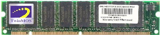
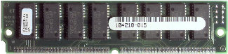
Approx. 5.375ö x 1.375 The DIMM is larger than either of the SIMMs. They contain 168 pins on the bottom of the circuit board. There are two notches on the bottom of the board and they must be aligned properly in order for them to be inserted. These memory modules are inserted one at a time unlike the SIMMs, which have to be inserted in pairs in 64 bit systems. 168-pin DIMMs are available in FPM, EDO, PC66, PC100 and PC133. The number of chips on a 168-pin DIMM may vary, but they have 84 pins on the front and 84 pins on the back for a total of 168.
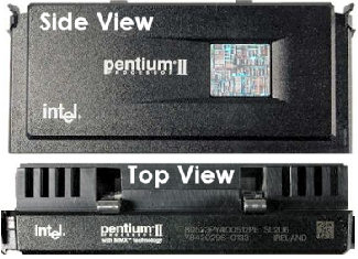
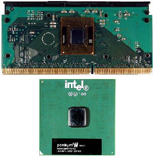
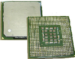
INTEL PENTIUM II
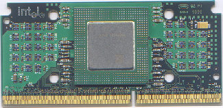
Slot 1 SECC 242 pin Single Edge Contact Cartridge Clock speed: 233 ¢ 450 MHz Front Side Bus speed: 66 ¢ 100 MHz L1 Cache: 16KB instruction, 16KB data L2 Cache: 512KB half-speed cache. Manufacturing: 0.35 micron ōKlamathö (233-300 MHz). 0.25 micron ōDeschutesö (300-450 MHz). Number of Transistors: 7.5 millions Due to the difficulty in manufacturing the Pentium Pro with on-chip L2 cache, Pentium II moved the L2 cache to an external cache reside in the ōSlot 1ö package. L1 Cache is doubled, and added the MMX instructions. 100 MHz front side bus is introduced after 350 MHz models.
1999 - 2000
INTEL PENTIUM III (Katmai)
Slot 1 SECC 242 pin Single Edge Contact Cartridge Clock Speed: 450 ¢ 600 MHz Front Side Bus Speed: 100 ¢ 133 MHz L1 Cache: 16KB instruction, 16KB data L2 Cache: 512KB half-speed cache. Manufacturing: 0.25 micron. Number of Transistors: 9.5 millions Summary: Same as Pentium II with added new SSE SIMD instructions. The ōBö model introduces 133 MHz front side bus.
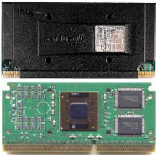
INTEL PENTIUM III (Coppermine)
Slot 1 SECC 242 pin Single Edge Contact Cartridge And also available in Socket 370 FC-PGA Flip Chip Pin Grid Array Clock Speed: 600 ¢ 1000 MHz Front Side Bus Speed: 100 ¢ 133 MHz L1 Cache: 16KB instruction, 16KB data L2 Cache: 256KB full-speed On-die cache. Manufacturing: 0.18 micron. Number of Transistors: 28 millions Major improvements from the original Pentium III, the L2 cache is now fully integrated onto the CPU die, and the L2 datapath, Associative, and Latency are also improved. The later model also revert back to the more conventional FC-PGA socket model from Slot 1.
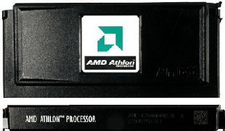
AMD ATHLON K7 (Pluto, Orion)
Slot A 242 pin SECC Clock Speed: 500 ¢ 1000 MHz Front Side Bus Speed: 100 MHz double data rate. L1 Cache: 64KB instruction, 64KB data L2 Cache: 512KB external cache. Manufacturing: 0.25 micron (Pluto). 0.18 micron (Orion) Number of Transistors: 22 millions The first processor based on the K7 architecture. The L2 cache is located on the external module similar to PII/III(katami) and runs at 1/2,3/5, 1/3 of the core clock speed.
AMD ATHLON K7 (Thunderbird)
Socket A 462 pin Clock Speed: 650 ¢ 1400 MHz Front Side Bus Speed: 100/133 MHz double data rate. L1 Cache: 64KB instruction, 64KB data L2 Cache: 256KB on-die cache. Manufacturing: 0.18 micron. Number of Transistors: 37 millions Similar to the improvement Intel made with the Coppermine core, the thunderbird integrates the L2 cache into the processor die and running at full core clock speed. The thunderbirds produced in Dresden fab are also the first x86 CPU to use the copper-interconnect.

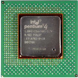
INTEL PENTIUM 4 (Willamette)
Socket 423 and Socket 478 Clock Speed: 1300 ¢ 2000 GHz Front Side Bus Speed: 100 MHz quad data-rate. L1 Cache: 12K micro-op instruction, 8KB data L2 Cache: 256 KB full speed On-die. Manufacturing: 0.18 micron. Number of Transistors: 42 millions. The first CPU core with the new Netburst(P68) architecture. Because of the fact that it is still manufactured using the older 0.18 micron technology. The die of this CPU is extremely large.
2001
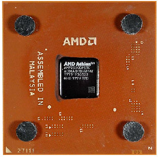
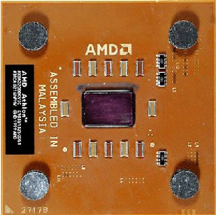
AMD ATHLON XP (Palomino)
Socket A 462 pin Clock Speed: 1333(1500+) ¢ 1.67(2100+) MHz Front Side Bus Speed: 133 MHz double data rate. L1 Cache: 64KB instruction, 64KB data L2 Cache: 256KB on-die cache. Manufacturing: 0.18 micron. Number of Transistors: 37.5 millions The Palomino core is mainly a reworked Thunderbird core to reduce power consumption with added thermal diode. The core also incorporated the SSE instructions, increased TLB, and a data prefetch unit. Externally, the CPU is packaged using the OPGA array (ie. Plastic) instead of Ceramic.
2002
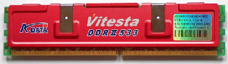
DDR SDRAM 184pin - Data is processed twice in each FSB clock cycle.
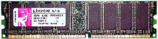
Approx. 5.375ö x 1.375 But what's all the 133/266, 166/333 and 200/400 numbers you ask? And what about PC2100, PC2700 and PC3200? What's it all mean? If the RAM is quoted as DDR266, then this means the data is running 2 x 133 where 133 is the core Front Side Bus speed. But wait, the RAM says it is PC2100. What's that? 2100 is a new naming standard for speed or throughput of data. It equals the theoretical speed of the RAM in MegaBytes per second. Here's a table to help explain: PC1600 Data at 200MHz Theoretical transfer rate of DDR200 Clock 200MHz core FSB 1.6Gigabyte per second _________________________________________________________________ PC2100 Data at 266MHz Theoretical transfer rate of DDR266 Clock 133MHz core FSB 2.1Gigabyte per second _________________________________________________________________ PC2700 Data at 333MHz Theoretical transfer rate of DDR333 Clock 166MHz core FSB 2.7Gigabyte per second _________________________________________________________________ PC3200 Data at 400MHz Theoretical transfer rate of DDR400 Clock 200MHz core FSB 3.2 Gigabyte per second
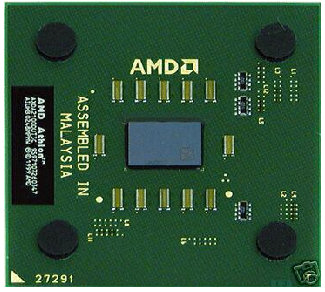
AMD ATHLON XP (Thoroughbred)
Socket A 462 pin Clock Speed: 1466(1700+) ¢ 2.1(2800+) MMz Front Side Bus Speed: 133/166 MHz double data rate. L1 Cache: 64KB instruction, 64KB data L2 Cache: 256KB on-die cache. Manufacturing: 0.13 micron. Number of Transistors: 37.5 millions Summary: Simply a die shrunk of the Palomino core to 0.13 micron. All the functionalities remains unchanged.
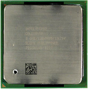
INTEL PENTIUM 4 (Northwood)
Socket 478 Clock Speed: 1600 ¢ 3066 MHz Front Side Bus Speed: 100 MHz or 133 MHz quad data-rate. L1 Cache: 12K micro-op instruction, 8KB data L2 Cache: 512 KB full speed On-die. Manufacturing: 0.13 micron. Number of Transistors: 55 millions. The second CPU based on the Netburst architecture. The processor is now manufactured using copper 0.13 micron technology. The L2 cache has been double in size to 512KB. However, the die size is still smaller than the Willamette.
2003
AMD ATHLON XP (Barton)
Socket A 462 pin Clock Speed: 2500+ ¢ 3000+ MHz Front Side Bus Speed: 166 MHz double data rate. L1 Cache: 64KB instruction, 64KB data L2 Cache: 512KB on-die cache. Manufacturing: 0.13 micron. Number of Transistors: 54.3 millions Same as Thoroughbred core Athlon XP with an increase L2 cache to 512KB.
2004
INTEL PENTIUM 4 (Prescott)
Socket 478 Clock Speed: to 3.6GHz Front Side Bus Speed: 200 MHz quad data-rate. L1 Cache: 16K L2 Cache: 1MB full speed On-die. Manufacturing: 0.09 micron or 90nm. Number of Transistors: 125 millions. DidnÆt show significant performance improvement over the Northwood core despite new micron size and 70 million extra transistors.
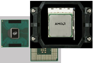
Later generation Socket 478 Pentium 4 processors were the
first to implement Intel's Hyper-Threading Technology, which
allowed for applications to be run in parallel, thus improving
the performance of the system. Although not nearly as strong,
the concept is similar to having a dual processor system or
dual-core processor, as systems with Hyper-Threading enabled
processors can handle intensive applications much easier than
the same system without Hyper-Threading.
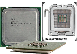
INTEL PENTIUM 4 (Grantsdale & Alderwood)
Socket 775 Clock Speed: to 3.6GHz Front Side Bus Speed: 200 MHz quad data-rate. L1 Cache: 16K L2 Cache: 1MB full speed On-die. Manufacturing: 0.09 micron or 90nm. Number of Transistors: 125 millions. New LGA ¢ Land Grid Array socket The Celerons in Socket T only support a 533 MHz frontside bus (Celeron D), and the Pentium 4s support both an 800 MHz frontside bus and a new 1066 MHz (266 MHz x 4) frontside bus. Speeds of the processors can range from under 3 GHz
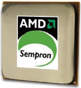
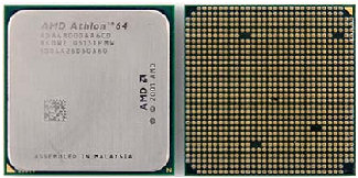
AMD ATHLON SEMPRON (ClawHammer)
Socket 754 pin  64Bit

Clock Speed: SP 3100+ / 1.80GHz
Front Side Bus Speed: 166 MHz double data rate.
L1 Cache: 64KB instruction, 64KB data
L2 Cache: 256KB on-die cache.

Manufacturing:
0.13 micron.
Number of Transistors: 68.5 million

This socket is the cheap socket for 64 bit Athlons.
Motherboards with this socket only support single
channel memory configurations which will slow
down performance.
AMD ATHLON 64 (939 Pin) (SledgeHammer)
AMD ATHON FX (940 Pin) (Opteron)
Socket 939 pin  64 Bit/32 Bit

Clock Speed: 3500+ / 2.20GHz
Front Side Bus Speed: 200 MHz quad-data rate with
Hyper Transport (Effective 1600MHz FSB).
L1 Cache: 64KB instruction, 64KB data
L2 Cache: up to 1024KB on-die cache.

Manufacturing:
0.13 micron.
Number of Transistors: 105.9 million transistors
2005
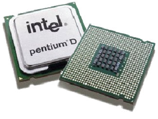
INTEL PENTIUM D (Smithfield - Dual Core)
Socket 775 LGA

Clock Speed: to 2.8 - 3.2 GHz
Front Side Bus Speed: 233 MHz quad data-rate.
L1 Cache: 16K
L2 Cache: 2x1MB full speed On-die.

Manufacturing: 0.09 micron or 90nm.
Number of Transistors: 230 millions.

Does work in existing socket 775 motherboards. Clocks
have reached a temporary ceiling.  Dual channel and
multiple data rates are the existing future.

Dual Core, Dual Channel, Hyper Threading,
Hyper Transport, Pipelines - All using more channels for
moving data about without increasing clock speeds.
AMD 64 x2 (Winchester - Dual Core)
Socket 939 pin  64 Bit/32 Bit

Clock Speed: 4500+
Front Side Bus Speed: 200 MHz quad-data rate with
Hyper Transport (Effective 1600MHz FSB).
L1 Cache: 64KB instruction, 64KB data
L2 Cache: up to 2x1024KB on-die cache.

Manufacturing:
0.09 micron or 90nm.
Number of Transistors: 233.2 million transistors
2006
DDR2 SDRAM 240pin - Data is processed four times in each FSB core clock cycle effectively Quad Data Rate.
Approx. 5.375ö x 1.375 The advantage of DDR2 over DDR SDRAM is the ability for much higher clock speeds, due to design improvements. The difference of DDR2 to DDR is a doubled bus frequency for the same physical clock rate, thus doubling the effective data rate another time. PC2-3200 Data at 400MHz Theoretical transfer rate of DDR200x2 Clock 100MHz core FSB 3.2 Gigabyte per second _________________________________________________________________ PC2-4200 Data at 533MHz Theoretical transfer rate of DDR266x2 Clock 133MHz core FSB 4.267 Gigabyte per second _________________________________________________________________ PC2-5300 Data at 667MHz Theoretical transfer rate of DDR333x2 Clock 166MHz core FSB 5.333 Gigabyte per second _________________________________________________________________ PC2-6400 Data at 800MHz Theoretical transfer rate of DDR400x2 Clock 200MHz core FSB 6.4 Gigabyte per second DDR2 DIMMs are not backwards compatible with DDR DIMMs. The notch on DDR2 DIMMs is in a different position than DDR DIMMs, and the pin density is slightly higher than DDR DIMMs. DDR2 is a 240-pin module, DDR is a 184-pin module
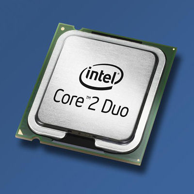
Current Range of INTEL and AMD Dual Core
Intel Core 2 Duo
Code name |
Cache |
Speed |
Throughput |
FSB |
E6850 |
4 MB L2 |
3.00 GHz |
1333 MHz |
166 MHz x 4 HT |
E6750 |
4 MB L2 |
2.66 GHz |
1333 MHz |
166 MHz x 4 HT |
E6700 |
4 MB L2 |
2.66 GHz |
1066 MHz |
133 MHz x 4 HT |
E6600 |
4 MB L2 |
2.40 GHz |
1066 MHz |
133 MHz x 4 HT |
E6550 |
4 MB L2 |
2.33 GHz |
1333 MHz |
166 MHz x 4 HT |
E6540 |
4 MB L2 |
2.33 GHz |
1333 MHz |
166 MHz x 4 HT |
E6420 |
4 MB L2 |
2.13 GHz |
1066 MHz |
133 MHz x 4 HT |
E6400 |
2 MB L2 |
2.13 GHz |
1066 MHz |
133 MHz x 4 HT |
E6320 |
4 MB L2 |
1.86 GHz |
1066 MHz |
133 MHz x 4 HT |
E6300 |
2 MB L2 |
1.86 GHz |
1066 MHz |
133 MHz x 4 HT |
E4500 |
2 MB L2 |
2.20 GHz |
800 MHz |
200 MHz x 4 |
E4400 |
2 MB L2 |
2.00 GHz |
800 MHz |
200 MHz x 4 |
E4300 |
2 MB L2 |
1.80 GHz |
800 MHz |
200 MHz x 4 |
Complete list of Core 2 Duo from Intel
Complete list of Core 2 Quad CPUs from Intel
Process Technology:, 65nm (.065-micron)
Approximately 291M Transistors. Core 2 Duo "Conroe"
 AMD 64x2 AM2
3800+ 2.0GHz
4200+ 2.2GHz
4600+ 2.4GHz
5000+ 2.6GHz
FX-62 2.8GHz
Process Technology:, 90nm (.09-micron)
Approximate Transistor count:, 153.8 million.
AMD 64x2 AM2
3800+ 2.0GHz
4200+ 2.2GHz
4600+ 2.4GHz
5000+ 2.6GHz
FX-62 2.8GHz
Process Technology:, 90nm (.09-micron)
Approximate Transistor count:, 153.8 million.
For the past few years, Intel's desktop processors have been playing second fiddle to AMD's Athlon 64 in a number of ways.
Both single and dual-core variants of the Athlon 64 have been at the top of most benchmark charts essentially since their
introduction, and AMD's processors have been more energy efficient as well. Conversely, since the introduction of the
Prescott core, Intel's processors have earned a somewhat notorious reputation for running hot and consuming more
than their fare share of power.
This scenario has played out since September of 2003, when AMD first released the Athlon 64 FX-51.
Intel's Core 2 Duo and Core 2 Extreme are here, and they seem to be everything Intel promised and then some.
The Core 2's 4-issue core, shorter pipeline, Smart Memory Access and Advanced Smart Cache technologies make Intel the
performance leader once again. It was a tough few years for Intel, as AMD's Athlon 64, FX, and X2 processors
outperformed their products almost across the board. But Intel isn't playing second fiddle to AMD anymore. Make no
mistake, the Core 2 Duo and Core 2 Extreme are very real, and their performance is undeniable.
AMD Phenom CPU Quad and Triple Core
2008
DDR3 SDRAM 240pin
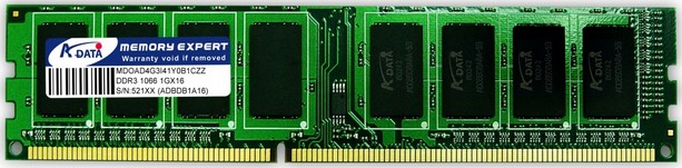
Approx. 5.375ö x 1.375 DDR3 modules can transfer data at the effective clock rate of 800¢1600 MHz using both rising and falling edges of a 400¢800 MHz I/O clock. In comparison, DDR2's current range of effective data transfer rate is 400¢800 MHz using a 200¢400 MHz I/O clock, and DDR's range is 200¢400 MHz based on a 100¢200 MHz I/O clock. To date, the graphics card market has been the driver of such bandwidth requirements, where fast data transfer between framebuffers is required.